Lotiskorea Newsletter Vol. 26
|
|
|
Protochips announces the global availability of the AXON HFR High Frame Rate module for studying the high-speed dynamics of materials using Gatan Inc. IS cameras!
“Designed to work quickly and efficiently with large datasets, scientists now have a revolutionary capability to study applications including ceramics, catalysis and electronic materials”, said David Nackashi, Co-founder and CEO, Protochips, Inc. “Identifying the exact moments of interest within these images and metadata is a ‘needle-in-a-haystack’ problem. AXON HFR makes...”
To read the full press release, visit https://lnkd.in/e39NVWyV. |
|
|
Researchers from Oak Ridge National Laboratory including Dr. Ondrej Dyck, Dr. Andy Lupini, Dr. Stephen Jesse, Dr. Sinchul Yeom and Dr. Mina Yoon automated the electron beam in a scanning transmission electron microscope to precisely drill the holes in the single graphene layer. They observed that as the temperature was increased, the diffusion rate of the single-atom vacancies induced by the beam was also increased untill the vacancies coalesced together (recombined) forming stable and immobilized structure such as chains of vacancies and larger holes. One would expect that increases the temperature would drive the knock-on displacement of carbon atoms but counterintuitively, researchers observed that at elevated temperatures, vacancy defects came together forming more stable defect structures stabilizing the defect configurations in graphene. This study enhances our understanding of defect evolution and dynamics in 2D materials which strongly influence their electronic properties.
Automated electron microscopy experiments were performed on Nion UltraSTEM US200 operated at 100 kV and equipped with a CFEG electron source and quadrupole-octupole (QO) type C₃/C₅ aberration corrector capable of compensating for all axial aberrations upto the fifth-order including fifth-order spherical aberration (C₅) and six-fold astigmatism (A₅). Probe convergence semi-angle of 30 mrad was used and the images were acquired in MAADF mode which is more dose-efficient as compared to HAADF. In-situ heating was performed using a Protochips Fusion in-situ heating holder.
Small holes spontaneously heal due to reintegration of carbon adatoms to the edges of the holes refilling the holes with structurally defected graphene. The effect is inversely proportional to the temperature and particularly at lower temperatures, the holes were disappeared quickly and were no longer been able to be observed after completion of a single drilling scan array as can be observed in the MAADF-STEM image-sequence.
Read the interesting findings published in Carbon.
https://lnkd.in/dyvzVpkV
|
|
|
Water radiolysis inside the liquid cell TEM caused by the highly energetic electron beam produces many molecules, ions and free radicals including eₕ⁻, H•, OH•, H₂, H₂O, and H₃O⁺, HO₂•, H₂O₂, HO₂⁻, HO₃⁻, HO₃•, O₂, O₂⁻, O₃•, O₃⁻, OH•, OH⁻, and O⁻, that drive the electron beam chemistry in liquid cell TEM experiments. As it can be seen, there are some reducing molecular species that drive reduction of metal salts to metal atomic clusters, some oxidizing species that can drive certain oxidation reactions and some acidic and alkaline species that could potentially drive etching of the nanoparticles in the solution under electron beam irradiation. However, the electron beam chemistry of different non-aqueous liquids such as ionic liquids is elusive.
Researchers including Prof. Rolf Erni from Empa have investigated the growth of gold nanoparticles in the ionic liquid 1-butyl-3-methylimidazolium chloride using in-situ scanning transmission electron microscopy triggered by heat and electron beam irradiation. They observed different growth mechanisms including isotropic growth, monomer attachment, particle coalescence and Ostwald ripening. The in-situ STEM experiments were performed on a Cₛ-probe-corrected Thermo Fisher Scientific Titan Themis microscope operated at 300 keV using a Protochips Fusion 500 in-situ heating TEM holder.
The Z-contrast image sequence demonstrates atomistic mechanisms of growth of gold nanoparticles by coalescence and by single-atom attachment mechanisms with subsequent particle relaxation in the ionic liquid at elevated temperature. Single atoms (small yellow dots) can be seen moving around the larger gold atomic clusters and nanoparticles.
Read the interesting paper published in the journal Micron.
https://lnkd.in/dQmyBhH9
|
|
|
📖 Would you also like to be able to bias nanomaterials while looking at them in real time? The authors of this newest publication did just that! These 2D Janus transition-metal dichalcogenides (TMDs) and alloyed TMDs are paving the way in electronic device innovation, boasting stellar electronic, optical, and mechanical properties. Yet, understanding issues like electrical breakdown due to structural failure remains paramount.
⚡️Using in situ biasing experiments with the FusionAX coupled with transmission electron microscopy (TEM), enabling atomic-scale insights into polymorphic molybdenum sulfide selenide (MoSSe) devices. The selenization temperature plays a pivotal role in material phase transitions, shaping the electrical and mechanical properties of MoSSe.
🔍️This study also explored the impacts of electron-beam irradiation and bias voltage, blending experiments and theory. Quantifying defect coverage and size provides crucial insights into material degradation behavior
🔬Last but not least, the authors employed Cs-corrected scanning TEM, to track the evolving morphology, revealing varying fracture patterns under high voltage applications. Understanding cracks and defects resulting from Joule heating sheds light on fracture types and sizes.
Want to read the entire paper?
Find it here!
https://lnkd.in/eECuvSjg |
|
|
📖 The authors of this newest publication have looked into using the FusionAX system on catalyst materials made from Pt/C. By comparing Pt/C synthesized conventionally (Pt/C_P) with Pt/C synthesized via ultrasound assisted Polyol Synthesis (Pt/C_U) under similar conditions, intriguing revelations emerged.
🔥Both catalysts had comparable Pt content and particle size; however, Pt/C_U exhibited superior uniformity and dispersion of Pt nanoparticles. Crucially, in high-temperature environments where nanoparticles tend to clump, in situ analyses unveiled that Pt/C_U showcased notably enhanced adhesion between Pt particles and the carbon support compared to Pt/C_P.
⌛️Ultrasound's influence on the carbon support sans the Pt precursor uncovered the generation of oxygen functional groups (C-O, C = O, and O-C = O) acting as anchoring sites for Pt particles in Pt/C_U. This finally showed that Pt/C_U had a heightened stability in electrochemical accelerated stress tests, highlighting its potential for durable performance in practical applications.
Want to read the entire work?
Find it here!
https://lnkd.in/etUhM2dG |
|
|
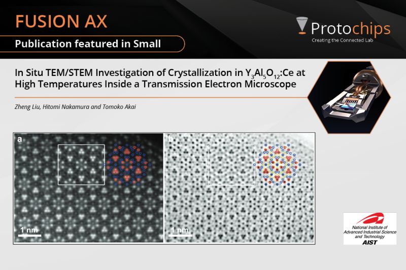
📖 Have you ever thought about investigating LED materials on the nanoscale using in situ transmission electron microscopy? The authors of this newest publication did! They used our FusionAX solution to look at the efficiency of Y3Al5O12:Ce (YAG:Ce) phosphors.
🔥Using the system, they were able to heat their nanocrystalline CeO2 material within the amorphous Y-Al matrix over 1000 °C. Intriguingly, at temperatures exceeding 900°C, the CeO2 particles dissolved entirely into the Y-Al oxide matrix. As the heat climbed beyond 1000°C, crystalline YAlO3 (YAP)-type particles emerged, accompanied by an Al2O3 phase in grain boundaries. Finally, the formation of YAG:Ce-type crystalline particles was observed above 1180°C.
🔬From there on, they used atomic-resolution energy-dispersive X-ray spectroscopy (EDS) elemental mapping to reveal more information of the nanomaterials. The doped cerium (Ce) atoms occupied the same atomic sites as yttrium (Y), unveiling crucial insights into the material's atomic arrangement.
Would you like to read the entire work? Find it here!
https://lnkd.in/ebQ9kez7' |
|
|
📖 In this newest publication, the authors used the electrical capabilities of the FusionAX system to look at the optoelectronic properties of fully processed red-emitting AlGaInP micro-diode devices
🔍️The quantum wells within the diode exhibited a fascinating behavior—they rested on a potential gradient until reaching the threshold forward bias voltage for light emission. At this critical point, these wells aligned at the same potential, a pivotal condition for efficient light emission.
📈Simulations mirrored these findings, showcasing the alignment of quantum wells at the same energy level upon reaching the threshold voltage. This alignment harbors electrons and holes primed for radiative recombination, facilitating light emission.
⚡️The application of off-axis electron holography emerges as a game-changing technique, enabling direct measurement of potential distribution in optoelectronic devices. This tool not only unravels device dynamics but also significantly enhances our ability to refine simulations and advance device performance.
Want to read the entire paper?
Find it here!
https://lnkd.in/gDduZ36D |
|
|
📖 In this study, published in Nature Communications, a low-dose imaging technique was used to delve deep into the phase structures (α, β, and γ) within CsPbI3 nanocrystals during in situ heating processes using our FusionAX system.
🔍️This cutting-edge approach enables us to pinpoint different phase structures and quantify thermal-induced phase distributions by measuring the rotation angles of PbI6 octahedrons at atomic resolution.
🔥The transition dynamics at a macro time scale by continuously imaging phase distributions within a single nanocrystal were studied. Witnessing the structural evolution of CsPbI3 nanocrystals at the particle level—morphological changes, compositional shifts—while escalating temperatures.
🔬What they saw? Atomic insights into the transition dynamics of perovskite phases. This unveils a prolonged transition process with discernible intermediate states and spatial distributions. It emphasizes the significance of considering these aspects in understanding structure-property relationships and optimizing device performance.
Want to read the full paper?
Find it here!
https:/https://lnkd.in/e9JrKmTK |
|
|
📖 In this recent study, the authors used our AtmosphereAX to witness real-time morphological and phase alterations at the oxide/metal interface of anodically formed NTs during annealing.
🔬They investigated samples both with and without the substrate, unraveling pivotal insights into substrate effects on NT phase changes.
🔍️With the substrate present, the oxide/metal interface revealed a fascinating bilayer structure. ART initiation was observed in the upper layer, while the bottom layer saw hydride and nitride precipitation. At temperatures surpassing 500°C, the substrate experienced spalling, losing its ordered morphology and crystallinity.
📈Surprisingly, when NTs were detached from the substrate, no evidence of ART or precipitation emerged. These revelations underscore the indispensable role of the titanium substrate in orchestrating morphological and phase transformations during annealing of NTs.
This study sheds light on the intricate relationship between titanium substrates and NT transformations, laying the groundwork for more informed design and application strategies in various industries.
Want to read the entire paper?
Find it here!
https://lnkd.in/eC8xUnKg |
|
|
문의
Email : hskim@lotiskorea.com
Tel : 010-2858-2798 |
|
|
|